SEQUENTIAL CIRCUITS
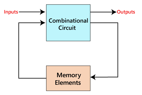
The sequential circuit is a special type of circuit that has a series of inputs and outputs. The outputs of the sequential circuits depend on both the combination of present inputs and previous outputs. The previous output is treated as the present state. So, the sequential circuit contains the combinational circuit and its memory storage elements. A sequential circuit doesn't need to always contain a combinational circuit. So, the sequential circuit can contain only the memory element.
In synchronous sequential circuits, synchronization of the memory element's state is done by the clock signal. The output is stored in either flip-flops or latches(memory devices). The synchronization of the outputs is done with either only negative edges of the clock signal or only positive edges.
The clock signals are not used by the Asynchronous sequential circuits. The asynchronous circuit is operated through the pulses. So, the changes in the input can change the state of the circuit. The asynchronous circuits do not use clock pulses. The internal state is changed when the input variable is changed. The un-clocked flip-flops or time-delayed are the memory elements of asynchronous sequential circuits. The asynchronous sequential circuit is similar to the combinational circuits with feedback.
FLIP FLOP
A circuit that has two stable states is treated as a flip flop. These stable states are used to store binary data that can be changed by applying varying inputs. The flip flops are the fundamental building blocks of the digital system. Flip flops and latches are examples of data storage elements. In the sequential logical circuit, the flip flop is the basic storage element. The latches and flip flops are the basic storage elements but different in working.
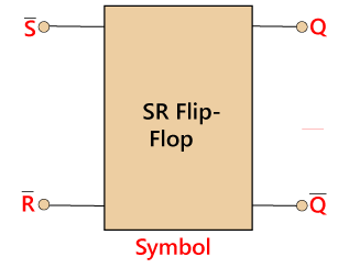
SR FLIPFLOP
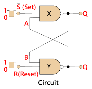
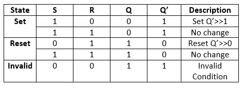
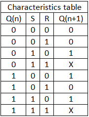
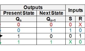
The SR flip flop is a 1-bit memory bistable device having two inputs, i.e., SET and RESET. The SET input 'S' set the device or produce the output 1, and the RESET input 'R' reset the device or produce the output 0. The SET and RESET inputs are labeled as S and R, respectively. The SR flip flop stands for "Set-Reset" flip flop. The reset input is used to get back the flip flop to its original state from the current state with an output 'Q'. This output depends on the set and reset conditions, which is either at the logic level "0" or "1".
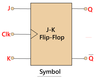
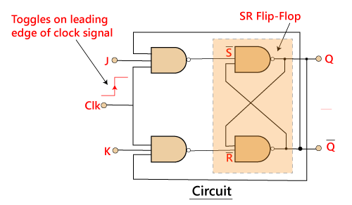
JK FLIPFLOP
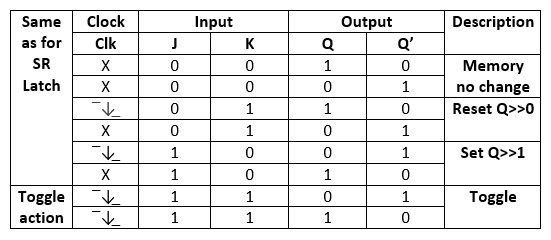
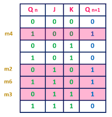
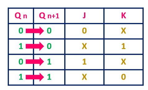
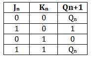
The JK flip flop work in the same way as the SR flip flop work. The JK flip flop has 'J' and 'K' flip flop instead of 'S' and 'R'. The only difference between JK flip flop and SR flip flop is that when both inputs of SR flip flop is set to 1, the circuit produces the invalid states as outputs, but in case of JK flip flop, there are no invalid states even if both 'J' and 'K' flip flops are set to 1. The JK Flip Flop is a gated SR flip-flop having the addition of a clock input circuitry. The invalid or illegal output condition occurs when both of the inputs are set to 1 and are prevented by the addition of a clock input circuit. So, the JK flip-flop has four possible input combinations, i.e., 1, 0, "no change" and "toggle". The symbol of JK flip flop is the same as SR Bistable Latch except for the addition of a clock input.
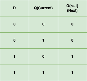
D FLIPFLOP
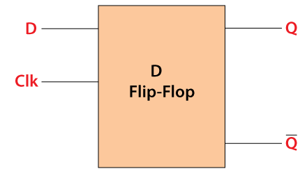
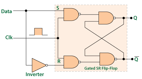
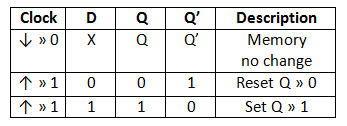
The D flip flop is the most important flip flop from other clocked types. It ensures that at the same time, both the inputs, i.e., S and R, are never equal to 1. The Delay flip-flop is designed using a gated SR flip-flop with an inverter connected between the inputs allowing for a single input D(Data). This single data input, which is labeled as "D" used in place of the "Set" input and for the complementary "Reset" input, the inverter is used. Thus, the level-sensitive D-type or D flip flop is constructed from a level-sensitive SR flip flop.
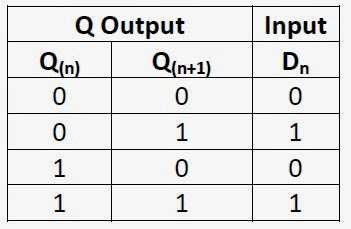
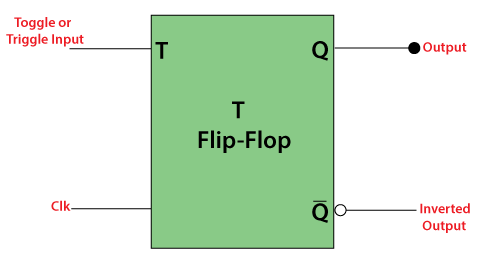
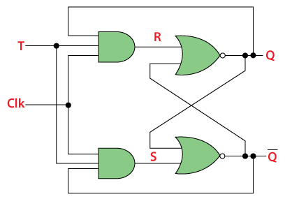
T FLIPFLOP
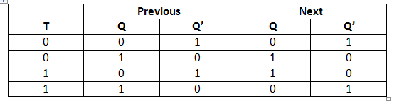
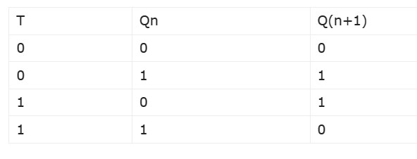
In T flip flop, "T" defines the term "Toggle". In SR Flip Flop, we provide only a single input called "Toggle" or "Trigger" input to avoid an intermediate state occurrence. Now, this flip-flop work as a Toggle switch. The next output state is changed with the complement of the present state output. This process is known as "Toggling"'.

SHIFT REGISTERS
A group of flip flops which is used to store multiple bits of data and the data is moved from one flip flop to another is known as Shift Register. The bits stored in registers shifted when the clock pulse is applied within and inside or outside the registers. To form an n-bit shift register, we have to connect n number of flip flops. So, the number of bits of the binary number is directly proportional to the number of flip flops. The flip flops are connected in such a way that the first flip flop's output becomes the input of the other flip flop.
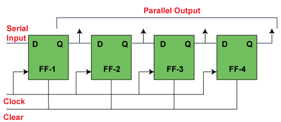
SISO REGISTER
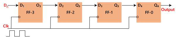
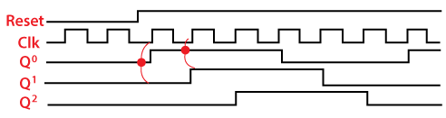
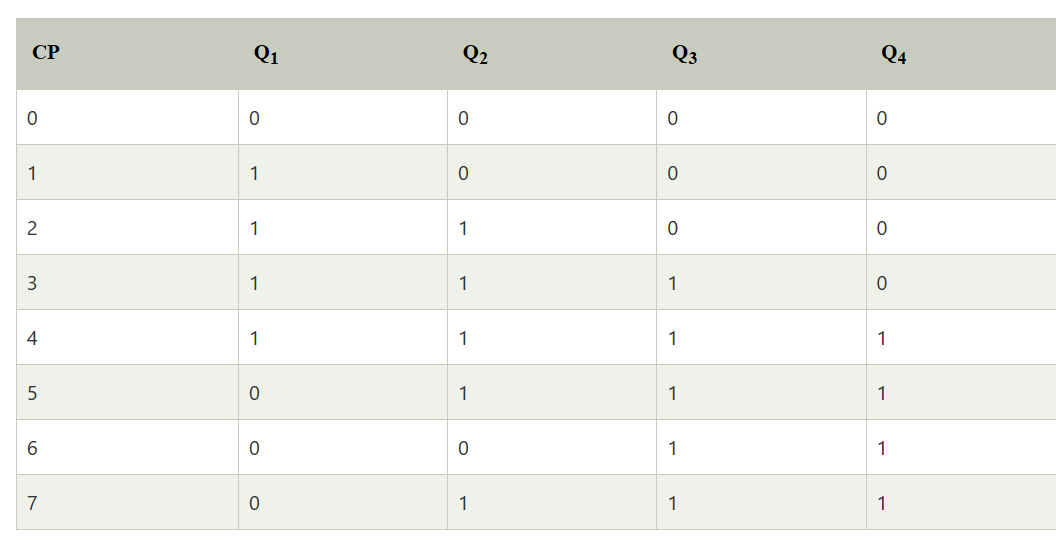
In "Serial Input Serial Output", the data is shifted "IN" or "OUT" serially. In SISO, a single bit is shifted at a time in either right or left direction under clock control. Initially, all the flip-flops are set in "reset" condition i.e. Y3 = Y2 = Y1 = Y0 = 0. If we pass the binary number 1111, the LSB bit of the number is applied first to the Din bit. The D3 input of the third flip flop, i.e., FF-3, is directly connected to the serial data input D3. The output Y3 is passed to the data input d2 of the next flip flop. This process remains the same for the remaining flip flops.
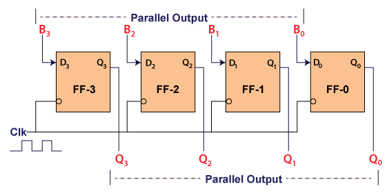
PISO REGISTER
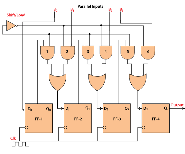
In the "Parallel IN Serial OUT" register, the data is entered in a parallel way, and the outcome comes serially. A four-bit "Parallel IN Serial OUT" register is designed below. The input of the flip flop is the output of the previous Flip Flop. The input and outputs are connected through the combinational circuit. Through this combinational circuit, the binary input B0, B1, B2, B3 are passed. The shift mode and the load mode are the two modes in which the "PISO" circuit works..
PIPO REGISTER
In "Parallel IN Parallel OUT", the inputs and the outputs come in a parallel way in the register. The inputs A0, A1, A2, and A3, are directly passed to the data inputs D0, D1, D2, and D3 of the respective flip flop. The bits of the binary input is loaded to the flip flops when the negative clock edge is applied. The clock pulse is required for loading all the bits. At the output side, the loaded bits appear.
SIPO REGISTER
In the "Serial IN Parallel OUT" shift register, the data is passed serially to the flip flop, and outputs are fetched in a parallel way. The data is passed bit by bit in the register, and the output remains disabled until the data is not passed to the data input. When the data is passed to the register, the outputs are enabled, and the flip flops contain their return value
BIDIRECTIONAL SHIFT REGISTER
The binary number after shifting each bit of the number to the left by one position will be equivalent to the number produced by multiplying the original number by 2. In the same way, the binary number after shifting each bit of the number to the right by one position will be equivalent to the number produced by dividing the original number by 2. For performing the multiplication and division operation using the shift register, it is required that the data should be moved in both the direction, i.e., left or right in the register. Such registers are called the "Bidirectional" shift register
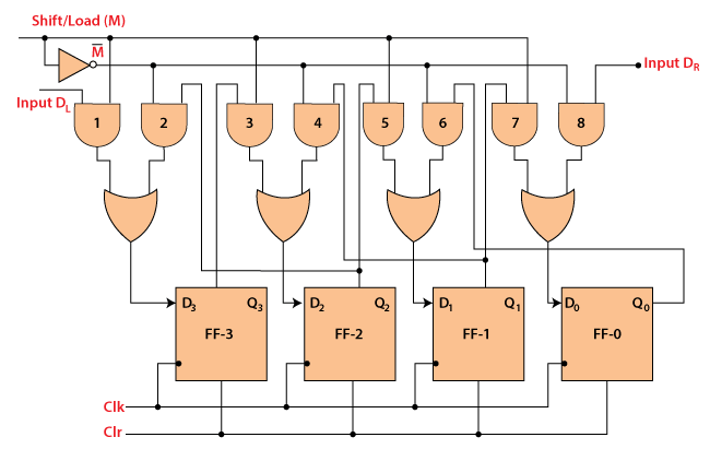
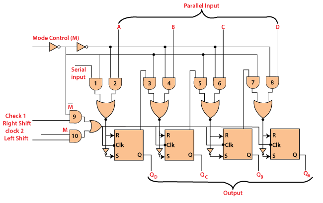
UNIVERSAL SHIFT REGISTER
A register where the data is shifted in one direction is known as the "uni-directional" shift register. A register in which the data is shifted in both the direction is known as "bi-directional" shift register. A "Universal" shift register is a special type of register that can load the data in a parallel way and shift that data in both directions, i.e., right and left. The input M, i.e., the mode control input, is set to 1 to perform the parallel loading operation. If this input set to 0, then the serial shifting operation is performed. If we connect the mode control input with the ground, then the circuit will work as a "bi-directional" register. The diagram of the universal shift register is given below. When the input is passed to the serial input, the register performs the "serial left" operation. When the input is passed to the input D, the register performs the serial right operation.
COUNTERS
A special type of sequential circuit used to count the pulse is known as a counter, or a collection of flip flops where the clock signal is applied is known as counters. The counter is one of the widest applications of the flip flop. Based on the clock pulse, the output of the counter contains a predefined state. The number of the pulse can be counted using the output of the counter
In the Asynchronous counter, the present counter's output passes to the input of the next counter. So, the counters are connected like a chain. The drawback of this system is that it creates the counting delay, and the propagation delay also occurs during the counting stage. The synchronous counter is designed to remove this drawback. In the synchronous counter, the same clock pulse is passed to the clock input of all the flip flops. The clock signals produced by all the flip flops are the same as each other.
RIPPLE COUNTER
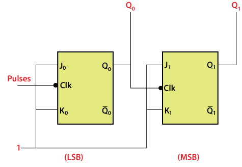
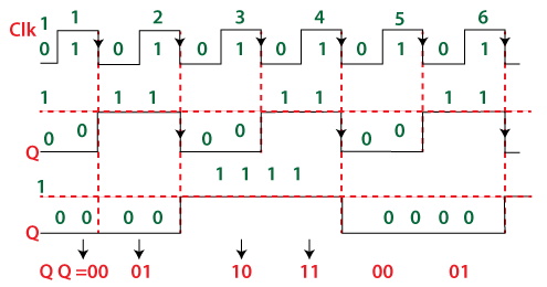
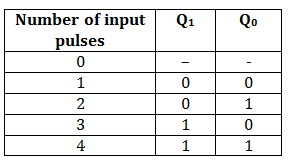
Ripple counter is a special type of Asynchronous counter in which the clock pulse ripples through the circuit. The n-MOD ripple counter forms by combining n number of flip-flops. The n-MOD ripple counter can count 2n states, and then the counter resets to its initial value.
The up-counter counts the states in ascending order.The down counter counts the states in descending order.The up and down counter is a special type of bi-directional counter which counts the states either in the forward direction or reverse direction. It also refers to a reversible counter.
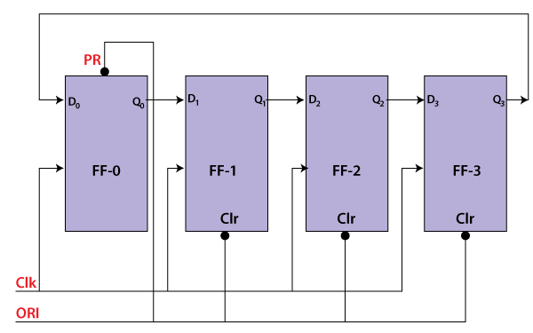
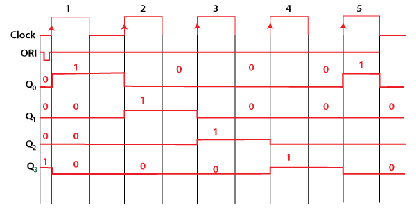
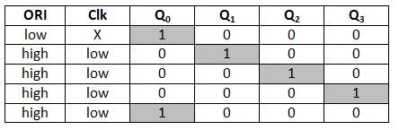
RING COUNTER
A ring counter is a special type of application of the Serial IN Serial OUT Shift register. The only difference between the shift register and the ring counter is that the last flip flop outcome is taken as the output in the shift register. But in the ring counter, this outcome is passed to the first flip flop as an input. All of the remaining things in the ring counter are the same as the shift register. No. of states in Ring counter = No. of flip-flop used
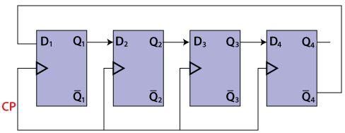
JOHNSON COUNTER
The Johnson counter is similar to the Ring counter. The only difference between the Johnson counter and the ring counter is that the outcome of the last flip flop is passed to the first flip flop as an input. But in Johnson counter, the inverted outcome Q' of the last flip flop is passed as an input. The remaining work of the Johnson counter is the same as a ring counter. The Johnson counter is also referred to as the Creeping counter.
No. of states in Johnson counter = No. of flip-flop used Number of used states=2n Number of unused states=2n - 2*n
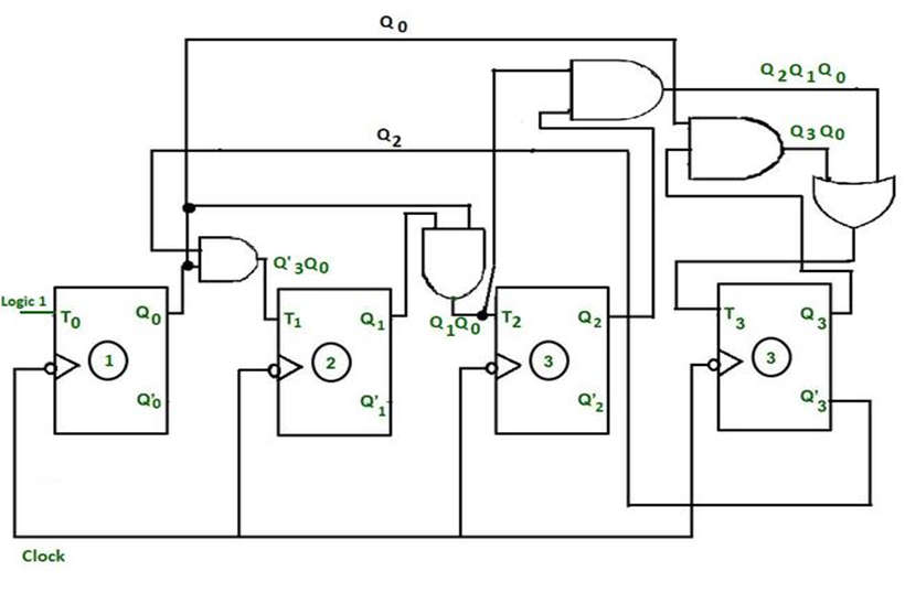
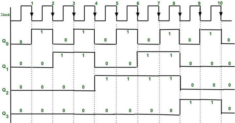
MOD-N COUNTER
A Modulus-M Counter is a counter in which M represents the number of states present. M = 2n(2 raised to power n), where ‘n’ is the number of flip-flops required to design the modulus-M counter. The modulus-6 counter, for example, has six states. The value of n, in this case, is 3. That means the module-6 counter requires three flip-flops to be designed.